August 10, 2021
Share on twitter Share on linkedin Share on reddit Share on emailBy Daniel Kriozere • Daniel is a Business Analyst at Lawrence Livermore National Laboratory and aspiring investor & advisor to clean-tech startups.
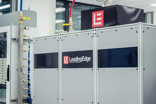
Even though the development of solar energy has come down in price and is critical to transitioning to clean energy, how clean are these solar panels? Rick Schwerdtfeger, CEO of Leading Edge, digs into this question from the perspective of the manufacturing process.
What problem are you trying to solve?
We’re trying to solve a couple of problems simultaneously, but the biggest one we’re trying to solve is to do our part to tackle climate change. Leading Edge is doing that by trying to enable a lower cost and better way to make silicon wafers for solar cells.
The second problem we’re trying to solve is the ability to make those solar wafers, cells, and modules in the US. We’ve lost that ability and we’re trying to rekindle that because our technology is advantageous enough that we can make silicon wafers in the US and have a cost advantage over the latest technology in Asia.
Why are you solving this problem?
I’m solving this problem for two reasons. First of all, I’ve had a keen interest in helping commercialize solar energy since I was in high school. My parents put a solar thermal system on our farm back in 1978, and I saw what an amazing job it did heating our old rural farmhouse in Illinois. At that time, nobody was doing that, especially out in the rural midwest.
As a result, when I went to school, I got a bachelor’s degree in physics and got a master’s degree in solar thermal energy. Unfortunately, at that point it was too late to try to work in that industry – it was dying after the Carter tax breaks were wiped out during the Reagan administration. So, I got my PhD in material science, specializing in photovoltaic materials, and then spent part of my early career studying solar energy. However, I left the solar field because there were not yet many jobs in the sector.
The core of what I was doing set me up to solve this problem today. I have been growing crystals, designing furnaces, and developing processes my whole career. When this opportunity came around to be back in the solar industry, using my skills as an entrepreneur, a manager, and as a scientist, it was the perfect alignment for me to now be able to tackle this problem again.
How did you end up joining Leading Edge?
Leading Edge’s technology began more than 12 years ago. Varian started working on this technology before they were bought by Applied Materials. Following that, the scientist that was working on it and an four-degreed MIT PhD engineer got together and spun it out of Applied Materials.
I entered the picture 4 years ago. I actually gave the company an SBIR grant for technology development when I was working at the National Science Foundation. I knew that it was right down my alley. It was a crystal growth, furnace development, and process development project – all the things that I had been doing for literally 30 years.
It was a couple of years later when Leading Edge was hiring a new CEO that I was asked by the board to apply. So, I left a federal government job to jump back into a startup – a world of craziness, challenges of raising money, helping to solve technical problems, hiring people, and all the other challenges associated with being an entrepreneur that I had been through with my previous startup.
What is the core technology of Leading Edge?
The core of the company lies on our ability to make single-crystal wafers horizontally by this kerfless ribbon growth process. We call it the FSM method, the Floating Silicon Method. FSM has never been commercialized anywhere in the world. There have been other vertical ribbon growth technologies commercialized. Pulling horizontal ribbon out of a melt offers a lot of advantages that vertical ribbons don’t. It’s also the first time a ribbon growth technology has successfully made single crystals of silicon wide enough to make modern solar wafers on. That’s the key differentiator for any other kerfless ribbon process – that we can make single crystals.
Fundamentally, we have to be really good at making these ribbons, cutting them into wafers, and doing it fast enough that the costs are low enough that we can beat any other competition. The cost is dependent on the rate at which you pull the ribbon out of the furnace, and if you can double the rate that you pull the ribbons, your cost goes down dramatically. One of our main R&D focuses is to figure out ways to pull these ribbons faster, which will enable us to attract more investors and make it easier to build new plants.
This is a very capital-intensive project because we will have to build a lot of furnaces to do this at scale. By 2030, we’ll need to have roughly 4,000 furnaces. We can ultimately get the cost of the capital equipment down to roughly 50% of what it is today, but it’ll probably take us five years to get there.
What are the benefits of the horizontal ribbon growth strategy versus vertical?
It’s better to talk about the advantages of the horizontal ribbon growth compared to the conventional way, which is a vertical growth process, but it’s not ribbon growth. Instead, it’s big round cylindrical ingot that is grown vertically out of a melt. That’s how all the single crystal silicon wafers in the world today are made. And it’s all done in China.
The advantage Leading Edge offers is that we don’t have saw wafers from big ingots – which turns almost half of the material into sawdust and can’t recycle because it’s too dirty. By having a kerfless process, there’s no sawdust created to make these ribbons because they’re formed at the correct thickness.
There’s only one company that I’m aware of that is trying to do a similar thing to Leading Edge. They are making a small number of wafers at a time, and they’re grown via a gas-phase process resulting in similar savings on kerf reduction and energy savings.
One of the nice things about being in such a high-growth market is that we could both be wildly successful, multi-billion-dollar companies and never have to really compete with each other. The market is so big and growing so fast that we don’t have to try to kill our competitor. We can encourage others to be successful in addition to us so the entire industry can grow and solar can increase its market share over conventional energy sources.
You touched upon this briefly, but how are you thinking about impact?
Reducing kerf waste does two things. It not only saves the raw material because you don’t have to use as much silicon per wafer, which saves cost, but it also saves a huge amount of energy, which can be globally impactful because the amount of energy it took to make that raw material that turned into sawdust by the other method is huge. It’s projected that by 2030, 5% of global CO2 emissions will be from the solar industry, most of which is coming from making the raw material to go into the furnaces. If everyone were to adopt our technology, the maximum impact would be cutting the emissions produced by the solar industry down to 2.5-3%.
What are current and future trends in the space?
The industry is on a trend of larger modules with higher power output. The path to higher output includes larger wafers. Also, innovation is making it possible to cut those wafers into halves or thirds to further increase power outputs by reducing resistive losses.
What that means for Leading Edge is that we need to be able to produce larger wafers over time. As a result, our R&D group is focused on not only pulling ribbons faster but pulling them wider so that we can cut bigger wafers out of them. This will help enable the entire industry to go to higher and higher power modules.
Outlook
The solar industry is booming, and it is going to keep accelerating – solar is here to stay, and Leading Edge is innovating to improve on energy generation in solar cells. In 2020, 82% of all new power capacity at the utility-scale was renewable. Leading Edge’s technology will only continue to help drive the prices of new solar projects down.
About The Author

Daniel Kriozere
Co-Founder at The ImpactMediumLinkedin-inBookmark
Daniel currently works at Lawrence Livermore National Laboratory. His original assignment was to maintain and update facility safety documentation for all facilities on-site, and perform risk analysis. Over time, his role has expanded to leading continuous improvement efforts through product management.
Concurrently, Daniel volunteers with Techstars, helping organize startup weekends, and with the American Institute of Chemical Engineers, organizing events on the local and national levels of the organization. He also volunteers with One World, and previously with Powerhouse Ventures, to source and screen startups for potential investment.
Daniel holds a BS in Chemical Engineering from UC Davis, and recently completed coursework in energy innovation from Stanford. His passion is at the intersection of sustainability, innovation, and business.