Fixing the solar industry’s dirty little secret
Solar energy is a growing percentage of global electricity generation and annual solar installations are projected to reach 1 terawatt by 2035, a ten-fold increase over the current total (2020). Rapid solar panel deployment is critical to keeping global temperatures to only 1.5 C above pre-industrial targets.
While solar panels don’t generate emissions during energy generation, solar panel manufacturing is extremely carbon-intensive. As the market exponentially grows over the next decade, solar panel manufacturing emissions are projected to reach over 1.5 gigatons of CO2/year – roughly equivalent to more than 6 percent of global emissions. Today, over 80 percent of this carbon footprint comes from manufacturing the silicon wafer – where the incumbent technology uses extremely energy-intensive furnaces to produce crystal ingots which are then wire-sawn into wafers, turning almost half of the ingot into useless saw dust.
Reducing Emissions by 50%
Leading Edge’s patented FSM™ process and manufacturing equipment can reduce the solar industry’s carbon footprint by over 50 percent. By producing a direct wafer without sawing and using extremely compact tools that consume 46 percent less energy, Leading Edge technology can dramatically reduce the up-front climate cost of transitioning to solar energy. Our mission at Leading Edge is to become the largest U.S.-based wafer manufacturer, and to enable a cost-competitive fully U.S. based PV supply chain.
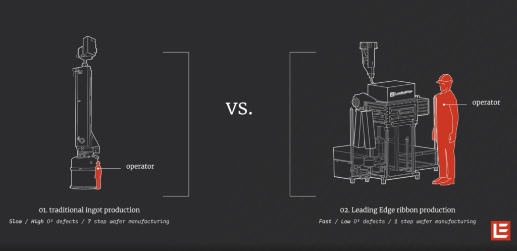
Eliminating Materials & Electrical Waste
Current Cz technology for creating single-crystal silicon wafers is extremely energy intensive and wasteful. By comparision, our technology requires a third of the energy as CZ technology and provides virtually no waste to develop single-crystal silicon wafers.
Large Cz-based furnances require 72 kW of power running consistently in order to melt large vats of silicon. After an ingot is drawn, wire sawing wastes 40 percent of the raw silicon as saw dust, or ‘kerf.’ Our technology requires only 25 kW of power to operate, has a meaningfully smaller footprint, and does not require wire sawing.